What are you looking for?
Chiplet & 3DIC Interconnect Design Solutions
Streamlined Chiplet and 3DIC Advanced Package Designs
Addressing Chiplet Design Challenges
Chiplets are small, specialized semiconductor components that can be integrated using high-speed standardized interfaces to form a complete system-on-chip (SoC), providing a modular alternative to traditional monolithic designs. By separating functions like processing, memory, and I/O into reusable building blocks, chiplets enable better performance, power efficiency, scalability, and cost optimization. This flexibility is driving rapid adoption across AI, HPC, data centers, networking, and automotive systems as designers move beyond the limits of monolithic scaling.
However, multi-die architectures introduce significant challenges, including complex interconnect structures, silicon interposers and bridges, advanced packaging elements like hatched ground planes, and the need for reliable die-to-die communication standards such as UCIe and BoW. These factors increase design complexity and validation requirements, making advanced simulation and AI-driven workflows essential. Solutions like Keysight’s Chiplet and 3DIC Interconnect Design tools address these challenges by enabling engineers to model, design, and validate interconnects earlier in the development cycle, reducing risk and accelerating time-to-market.
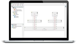
Chiplet 3D Interconnect Designer: Design and Optimize Chiplet Die-to-Die Channels in ADS
Chiplet 3D Interconnect Designer provides a fast and accurate design environment for die-to-die interconnects on silicon and organic bridges or interposers. It allows package and interconnect engineers to explore architectures and optimize interconnect channels before committing to a full package layout.
Key capabilities
- Physical channel design and optimization for chiplet interconnects
- Support for hatched and waffle ground planes
- Standard-driven bump maps for UCIe and BoW
- Fast mixed-domain channel modeling for early design exploration
- Guided, user-friendly design workflow
- Direct integration with Chiplet PHY Designer
3D Interconnect Designer: Comprehensive Design for Advanced Packages and 3DIC in Keysight, Cadence and Siemens workflows
3D Interconnect Designer (standalone software version) provides a flexible modeling and optimization environment for any advanced interconnect structure, including chiplets, stacked die, packages, and PCBs. It supports heterogeneous integration and works with existing EDA environments.
Key capabilities
- Modeling and optimization for vias, micro-bumps, transmission lines, and solder balls
- Support for stacked die, 3DIC architectures, and Custom bump map
- Hatched and waffle ground plane modeling
- Works with ADS or external EDA workflows


W3510E
Chiplet 3D Interconnect Designer
For Chiplet die-to-die channel design
- Design and optimize chiplet die-to-die interconnect channels
- Support for silicon bridges and interposers
- Hatched / waffle ground plane modeling
- Standard-driven bump maps for UCIe and BoW
- Integrated workflow with Chiplet PHY Designer
Best for Chiplet package designers optimizing interconnect channels

W9100E
3D Interconnect Designer
For Advanced 3D interconnect and package design
- Full 3D interconnect modeling for packages, chiplets, and PCBs
- Detailed modeling of vias, micro-bumps, transmission lines, solder balls. Hatched / waffle ground plane modeling
- Support for stacked die architectures
- Works with ADS or external EDA workflow
Best for Advanced package and 3DIC designers building complex heterogeneous systems
Want help or have questions?