


- Overview
- All Models
- Support
High-power device testing for today’s wide bandgap technologies
Keysight power device analyzers / curve tracers are purpose-built solutions for evaluating and characterizing high-voltage, high-current semiconductor devices. Combining accurate sourcing, fast measurement, and comprehensive analysis, these systems support critical tests for power transistors, diodes, IGBTs, and wide bandgap devices such as SiC and GaN. With scalable voltage and current ranges, integrated safety features, and intuitive software, Keysight solutions help accelerate development, improve device reliability, and streamline production testing. Request a quote for one of our popular configurations today. Need help selecting? Check out the resources below.
Wide measurement range
Test a variety of power semiconductors with source / measure capabilities up to 10 kV and 3000 A, accommodating both pulsed and steady-state operation modes.
Purpose-built solution
Characterize SiC and GaN components with fast switching performance and low on-resistance, ensuring reliable test results under real-world operating conditions.
Built-in protection features
Enhance test safety with integrated interlocks, compliance limit controls, and hardware safeguards designed to protect both the device under test and the operator.
Automation-ready software
Simplify power device validation with a curve tracing interface designed for fast setup, automated sweeps, and instant analysis of key parameters.
-
Maximum output current
200 A to 3000 A
-
Minimum current measurement resolution
10 fA
-
Number of channels
7 to 8
-
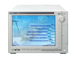
Supported measurements
DC I/V, Pulsed I/V, 1 kHz to 5 MHz CV, 3 kV high voltage CV, Gate charge (Qg), On-wafer I/V, Thermal test, Power loss calculation, Turn-on, Turn-off, Switching, Dynamic on-resistance, Gate charge, Reverse recovery, Dynamic voltage / current
-
Maximum output voltage
1200 V to 3 kV
Most popular configurations

Power Device Analyzer / Curve Tracer for Circuit Design
-semiconductors-by-double-pulse-testing-/Use-Case-Webpage-Hero-Banner-characterize-wide-bandgap-WBG-semiconductors-1600x900.png)
-semiconductors-by-double-pulse-testing-/Use-Case-Webpage-Hero-Banner-characterize-wide-bandgap-WBG-semiconductors-1600x900.png)
Dynamic Power Device Analyzer/Double Pulse Tester

Advanced Dynamic Power Device Analyzer / Double-Pulse Tester
Services and support
Innovate at speed with curated support plans and prioritized response and turn-around times.
Get predictable, lease-based subscriptions and full lifecycle management solutions—so you reach your business goals faster.
Experience elevated service as a KeysightCare subscriber to get committed technical response and more.
Ensure your test system performs to specification and meets local and global standards.
Make measurements quickly with in-house, instructor-led training, and eLearning.
Download Keysight software or update your software to the newest version.
Frequently asked questions
A power device analyzer or curve tracer is a specialized test system engineered to evaluate the static and dynamic behavior of power semiconductors such as MOSFETs, IGBTs, GaN HEMTs, and SiC devices. These systems are capable of sourcing and measuring high voltages (up to several kilovolts) and high currents (hundreds to thousands of amps), enabling comprehensive characterization of breakdown voltages, on-resistance, threshold behavior, saturation current, and more. Unlike standard SMU-based setups, power analyzers include high-energy pulse sources, safety interlocks, low-inductance layouts, and fast switching control to replicate real-world stress conditions. These capabilities are crucial for qualifying wide bandgap devices in applications such as EV inverters, industrial power conversion, and high-frequency power supplies, where failure or underperformance can lead to thermal damage, efficiency losses, or safety hazards.
Curve tracing is the process of sweeping voltage or current across a semiconductor device and measuring its response to generate I V curves, which reveal behavior across conduction, saturation, breakdown, and leakage regions. It is fundamental for characterizing nonlinear device physics and validating the safe operating area (SOA) of power devices.
These analyzers are designed to perform both static and dynamic measurements essential for device development and application validation. Key test types include:
- IV characteristics: Including output characteristics (Id-Vds), transfer characteristics (Id-Vgs), Rds(on), and gate leakage (Igss).
- Breakdown voltage (BVds): Non-destructive or destructive tests under controlled ramp conditions to determine avalanche capability.
- Gate charge (Qg) and input capacitance: Using dynamic charge-discharge profiles or pulse methods to evaluate switching energy and timing.
- Reverse recovery and body diode performance: To assess efficiency and loss during switching transitions.
- Pulsed measurements: Short-duration pulses prevent device self-heating and allow extraction of intrinsic properties like saturation current or transconductance.
- Thermal response: Via repetitive pulsed measurements or by integrating thermal control systems, these tests help evaluate device robustness under realistic load profiles.
Testing power devices involves potentially dangerous energy levels, making safety a critical design factor in power analyzers and curve tracers. These systems incorporate multiple safety layers, including:
- Hardware interlocks: Prevent high-voltage activation unless test enclosures are securely closed and grounded.
- Soft limits and compliance settings: Allow users to define maximum voltage/current thresholds, shutting off the test immediately if limits are exceeded.
- Arc detection and emergency shutdown: Some systems include fast-reacting arc sensors or programmable emergency stop buttons to protect both the user and the DUT.
- Low-inductance test fixtures and shielded enclosures: Reduce the risk of voltage overshoot or parasitic oscillations that can damage components or lead to hazardous conditions.
- Software safety checks: Test scripts often include pre-test validation steps, automatic ramping, and fault diagnostics to ensure repeatable, safe execution.
These safety mechanisms allow engineers to confidently test components with ratings up to 3 kV and 1500 A while maintaining high accuracy and avoiding catastrophic failure modes.
The right choice depends on the target device specifications, test parameters, and application domain. Key considerations include:
- Voltage and current range: For example, the B1506A supports up to 3 kV and 1500 A, making it suitable for automotive and industrial power devices. Lower-rated systems like the PD1000A may be ideal for consumer or telecom applications.
- Pulse width and speed: Faster pulses (e.g., <10 µs) are needed for GaN devices with low charge and high-speed switching. Systems with fine pulse control and minimal inductance are preferred for accurate dynamic behavior.
- Measurement resolution and timing: High-precision ADCs and nanosecond-scale timing resolution improve the ability to resolve fast transients, overshoot behavior, or diode recovery.
- Fixture compatibility and layout: Choose a system with appropriate DUT holders, Kelvin sensing fixtures, or customizable test benches based on your packaging (TO-247, modules, bare die).
- Software and automation: Engineers benefit from GUI-based control interfaces, parameter extraction tools, and scripting APIs for automated characterization, test repeatability, and data integration.
- Safety compliance and system certification: Ensure the analyzer meets lab safety requirements and includes fail-safes for operation in high-voltage environments.
Ultimately, system scalability, support for future device generations, and integration with thermal/EM simulation data can also factor into long-term testing strategies.
A curve tracer is optimized for fast graphical visualization of I V characteristics across wide ranges. An SMU provides precision sourcing and measurement with programmable control. Keysight’s Power Device Analyzer / Curve Tracer integrates both, combining the speed of a curve tracer with the accuracy and automation of SMU based systems.
A curve tracer performs voltage/current sweeps to generate I V characteristics, showing how a device behaves under different electrical stresses. An oscilloscope shows voltage vs. time and does not inherently characterize device parameters or nonlinear regions. Curve tracers are purpose built for semiconductor evaluation.
Curve tracers work by applying controlled voltage or current sweeps to a device while measuring and visualizing its nonlinear response. Modern curve tracers use SMU based sourcing, fast pulsed testing, and automated sweep control to reveal I V curves, capacitance behavior, gate charge, and dynamic switching characteristics essential for evaluating today’s power semiconductors.