How to Perform PCBA Chipset Tests

Testing PCBA chipsets with boundary scan
Testing printed circuit board assembly (PCBA) chipsets requires a boundary scan test to ensure accurate and reliable testing. As technology evolves, chipset testing becomes more challenging due to the complex interconnects, limited access points, and increasing component density. Boundary scan testing, as defined by IEEE 1149.1 and IEEE 1149.6 standards, enables access to internal nodes of digital components that observe and control signals at various points within the device through a shift-register-based architecture. Manufacturers are required to design the PCBAs according to the standards. That means manufacturers must connect boundary test cells to each pin of the PCBA.
Manufacturers must test the PCBAs using the in-circuit tester (ICT) and boundary scan analyzer consecutively on the production floor. The process starts with ICT inspecting the high-speed PCBA traces for any shorts or open traces. Once the PCBA passes the ICT test, it proceeds to the boundary scan test, which assesses high-speed interconnects and dual in-line memory module (DIMM) memory. Boundary scan offers an overall picture of the functionality within the PCBA while also enabling easy identification of manufacturing problems in specific pins.

PCBA chipsets test solution
See demo of PCBA chipset testing
This is a modal window.
Explore products in our PCBA chipset test solution
-

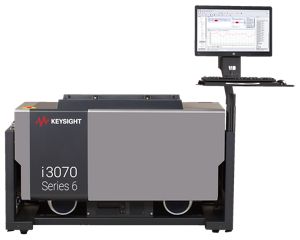
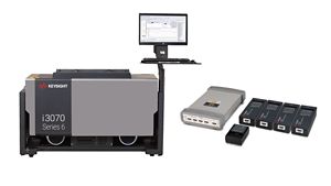
E9903G 4-Module ICT System, i307x Series 6
-
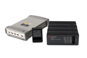
x1149 Boundary Scan Analyzer

Discover resources and insights
Additional resources for PCBA chipset testing
Related use cases


-
How to Integrate an In-Circuit Tester into Industry 4.0
Integrating an in-circuit tester into Industry 4.0 requires machines that can support IPC-CFX. Learn how to define communication protocols to ensure alignment with IPC-CFX standards.
Learn more

-
How to Speed Up Short Testing for High-Impedance Nodes
Short testing for high-density printed circuit board assemblies, which include high-impedance nodes, requires numerous impedance measurements between nodes. Learn how the enhanced short test algorithm enables faster and more accurate short testing.
Learn more
-
How to Test Passive Components without Access Points
Testing passive components on high-density PCBAs without test points necessitates grouping components into clusters and calculating impedance for precise testing. Learn how the enhanced cluster test solution automates the cluster generation process, ensuring efficient and accurate testing.
Learn more

Get in touch with one of our experts
Need help finding the right solution for you?