What are you looking for?
High-Speed Digital Design Software
Have confidence in your PCB designs before build-out
Designers need agility to handle today’s denser and more complex designs. Keysight EDA’s Advanced Design System (ADS) streamlines design verification and compliance through guided collaboration and standard-driven workflows.
Standards-Driven Workflows
- Video Player is loading.
This is a modal window.
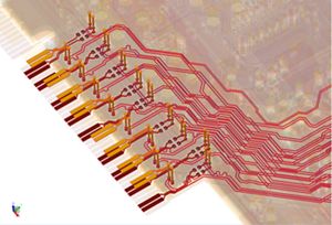
The media could not be loaded, either because the server or network failed or because the format is not supported.DDR 5/6 model extraction, signal integrity, and compliance verification
The ADS Memory Designer minimizes the effort required to generate IBIS-AMI models for receivers, extract accurate DDR channel electromagnetic (EM) models, and predict the margin to the eye mask at specific bit error rates.
Built-in support for the latest memory standards, DDR5 and GDDR6, and advanced signal integrity analysis capabilities with unwavering accuracy allow designers to set up end-to-end DDR analysis five times faster than before.
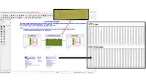

Chiplet die-to-die link signal integrity, and compliance verification
The ADS Chiplet PHY designer allows designers to predict the end-to-end link margin and compliance measures such as VTF for chiplet’s die-to-die interconnects.
It enables the forwarded clocking in UCIe to be accurately analyzed to consider the jitter tracking. Built-in support for standard-specific measurements makes verifying compliance with known chiplet standards easy.
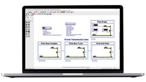
PCIe® 5/6 signal integrity, and virtual compliance test
The ADS System Designer for PCIe® automates the setup for multi-link, multi-lane, and multi-level (PAM4) PCIe systems using a smart design environment. The PCIe AMI modeler, which supports NRZ and PAM4 modulations, facilitates the quick implementation of PCIe systems.
The integrated simulation-driven compliance test solution can reduce design costs by minimizing design iterations and shortening time-to-market.
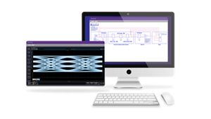
Signal Integrity for High-Speed Serial
Each new digital standard brings faster speeds and higher frequencies. Signal integrity engineers need to have confidence in their channel design, including optimal via design, managing crosstalk, signal loss, jitter, and equalization.
With advanced channel simulation in ADS, you can simulate for pulsed amplitude modulation (PAM-4, PAM-3, and PAM-N) signaling schemes. Complemented by fast and accurate signal integrity EM analysis, you can achieve 100% board success by catching critical errors before build-out.
View Lessons
Designing for Signal Integrity (10 min)
Power Integrity: More Than Just DC
With lower voltages, higher currents, and multiple supplies, power integrity issues can be difficult to troubleshoot and cost thousands of dollars to fix. Overcoming this challenge requires a cohesive design flow for frequency and time-domain analysis of power distribution networks (PDNs).
With Keysight’s power integrity (PI) design workflow, you can visualize the worst-case ripple caused by a dynamic load and engineer an optimum low-noise PDN.
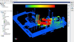
Multi-Physics Simulation
Denser electronics with intricate geometries, diverse materials, and high frequencies demand more advanced EM simulations.
Finite element method (FEM) tackles this complexity by handling irregular shapes, incorporating material properties, and enabling multi-physics (thermal or electromagnetic) analysis. It offers a holistic view of device performance, reducing physical prototyping risks.

High-Speed Digital Design: Go Deeper
Printed circuit boards (PCBs) get more complex and densely packed as technology advances and devices shrink.
Learn more with a deeper dive into standards-driven workflows, signal and power integrity with a curated selection of advanced topics.
Protect Your Innovation Investment


Electronic Design and High-Speed Digital Design FAQ
A guide to common questions and answers about electronic design, high-speed digital design, and standards-driven design
Want help or have questions?