How to Analyze Signal Integrity Using Layout Geometry

Identifying signal integrity issues through electrical performance scan
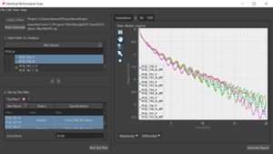
Achieving peak performance in high-speed printed circuit boards (PCB) requires verifying signal integrity (SI) compliance in all electrical traces with various performance specifications. Design engineers should perform quick signal integrity analysis to identify issues earlier in the circuit design and layout process. Doing so minimizes risk and maximizes PCB design productivity.
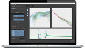
To speed up PCB prototype creation, designers can use layout geometry and simulation software. This software simulates the performance of a design and generates SI metrics such as trace impedance and delay, return and insertion loss, S-parameter analysis, and impedance time-domain reflectometry (TDR). Designers also need automation of routine tests and analysis automation to document the different revisions of simulations and results.

Signal integrity electrical performance scan solution
See demo of signal integrity EP-Scan
This is a modal window.
Explore products in our signal integrity EP-Scan solution
-

W9001E HSD Apps EP-Scan

Discover resources and insights
Additional resources for analyzing signal integrity issues using layout geometry
Related use cases


-
How to Determine DDR5 Controlled Trace Impedance
Addressing signal reflections in DDR5 designs requires properly designed controlled impedance traces. Learn how to use ODB++ files to generate impedance reports and eye diagrams for various data rates and adjust the control impedance to meet specifications.
Learn more

-
How to Accelerate High-Speed Digital Compliance Testing
Accelerating high-speed digital compliance test requires offloading data processing and reporting to external high-performance servers. Learn how to attain compliance results faster by offloading data processing from your oscilloscope onto high-performance computing resources that process data in parallel.
Learn more
-
How to Automate Supercapacitor Testing
Testing a supercapacitor on a printed circuit board assembly (PCBA) requires measuring its equivalent series resistance (ESR) and capacitance during the in-circuit test (ICT). Learn how to automate this process with intelligent program generation, DC electronic load, and a source measure unit into an ICT to accelerate supercapacitor testing.
Learn more

Get in touch with one of our experts
Need help finding the right solution for you?