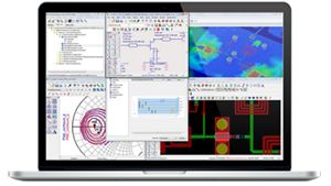
Key benefits of PIPro include:
- Speed and Accuracy - The EM technologies in PIPro are tuned specifically for Power Integrity (PI) applications, they are much faster and more efficient than general purpose EM tools.
- Designed for Usability - PIPro shares a common graphical user interface (GUI) in Advanced Design System (ADS) that is architected specifically for PI analysis. Navigating and setting up EM simulations on complex PCBs is made fast and simple with a net-driven use model. With the high-capacity solvers in PIPro, it is no longer necessary to spend hours manually simplifying designs, such as cookie-cutting and removing layers and nets, that is typically done with general purpose EM tools. Also, setting up EM ports and solver settings is much more automated than in general purpose EM tools.
- Cohesive Work Flow - With one common environment for both SI and PI analyses one setup can be easily copied from one analysis-type to another. Resulting EM models transfer seamlessly back to schematic for further simulation with Transient and Channel simulators. This flow eliminates the need to switch between different point tools, saving valuable engineering time.
PIPro provides power integrity analyses of your power distribution network (PDN), including DC IR drop analysis, AC impedance analysis and power plane resonance analysis. PIPro utilizes a common setup and analysis environment within Advanced Design System (ADS).
Feature Capability List
- DC IR Drop including losses in ground planes.
- Results overview with Voltage, Current, Current density per pin, via, layer, VRM and sinks.
- Results 'Compare-to', allowing easy comparison between results from different simulations.
- Voltage, Current Density and Power Loss visualization.
- Easy 'copy-to' command to move current setup to new setup type (e.g. IR Drop to IR Drop Electro-Thermal).
- Comprehensive output report format.
- DC IR Drop Electro-Thermal.
- Thermal-Only mode.
- Wizard tools for synthesis of thermal parameters.
- PDN Z-impedance Simulation.
- E & H-field visualization.
- Real-time PDN impedance update (changing decap models doesn't need a new EM sim).
- Mesh Domain Optimization (optimally reduces mesh size to solve).
- Decap Optimization for Bill of Materials (reduce number of decaps, number of vendors, cost etc).
- Power Plane Resonance Simulation.
- Python scripting interface.
- Power Tree results view.
PIPro Work Flow
The PIPro work flow includes design import, analysis setup, simulation, analyses and automatic schematic generation for further simulation.
Design Import
PCB layout designs can be imported to ADS using ODB++, .brd (Cadence Allegro) and ADFI formats. Once in ADS, the design is opened in the SIPro / PIPro analysis environment where it is viewed, zoomed and rotated in 3D.
PIPro Analysis Setup
Select the Voltage Regulator Modules (VRMs), components and sinks that you want to include in the analysis. For AC analysis, specify component models to be used for decoupling capacitors (decaps)
PIPro Simulation
The following analyses can be performed in PIPro:
DC IR Drop analysis
- Voltage delivered to each sink, and failures based on user-defined tolerances.
- Current flow through each via, and failures based on user-defined maximum values.
- 3D voltage distribution plot
- 3D current density plot
- 3D power loss density plot
- Power tree results and report generation
DC IR Drop Electro-Thermal
- Fully-automated, integrated Electrical-Thermal-Electrical iterative simulation.
- Easily copy existing DC IR Drop simulation setup to new Electro-Thermal simulation.
- Visualize a list the temperature of planes, pins and vias.
- Most accurate representation of DC IR Drop results by taking into account local resistivity changes due to heating.
- Test potential cooling solutions such as increasing the heatsink size, or increasing airflow.
- Additional Thermal-only simulation, gives the user the ability to perform thermal floor planning.
AC PDN impedance analysis
- PDN impedances vs. frequency
- S-parameter model extraction of PDN
- 3D field plots and current density plots
- Decap tuning – quickly see effects of changing decap values without resimulating.
Decap Optimization for Reducing Bill of Materials
Reference designs for many ICs provide a comprehensive list of decaps that should be placed on the PDN for best performance and reliability. This doesn't take into account the specific constraints that the designer may have on their PCB (size and layer count). Often there is not enough space around the IC and below the IC, to place all of the decaps, leaving the layout engineer to place the remaining components wherever they fit on the PDN. Decap Optimization in PIPro can take all the decaps as laid out on the board, and search for the optimal solution that meets the desired target impedance profile.
The user can define an optimal solution, by specifying weighted criteria such as:
- # of decaps
- # of unique models
- # of vendors
- Cost
The optimization is fast, by nature of the intelligent algorithms, and the fact that changing decap models does not require a re-computation of the EM solution. The optimization results are presented a list of candidate solutions that meet the target impedance, and are ranked according to the weighted criteria. For each candidate solution, the user can view the PDN Z-impedance vs target impedance, to quickly decide upon the best mix of performance and cost-reduction.
Power plane resonance analysis
- Self-resonant frequencies and quality factors for the PDN
- 3D field plots
Learn more about Advanced Design System (ADS) Simulation Elements

